
Our related videos
Knowledge
Advantages of ultra-thin copper foil and mSAP process for manufacturing fine-line circuits on IC carrier boards
Introduction of Ultra Thin Copper Foil:Ultra-thin copper foils are usually referred to as copper foils with a thickness of less than 9um. Since this kind of ultra-thin copper foil is too thin and light, a thicker layer of carrier copper foil of about 15-18um is usually added to increase its support.
Nowadays, it is mainly used in the manufacture of high-end PCBs, including IC carrier boards, Coreless substrates, and so on.
Topnano's Ultra Thin Carrier Copper Foil consists of 18um carrier copper foil and 3μm/5μm ultra thin copper foil with a Releasing Layer in between. Topnano's ultra-thin carrier copper foils are easy to peel off, have extremely low surface roughness (Rz<2um), and have good etchability.
mSAP Modified Semi-Additive Process Improves PCB Etch Yield Problems and Saves Manufacturing Costs:
" mSAP" is an acronym for "Modified Semi-Additive Process", which refers to the inner core of BT boards. The modified semi-additive process improves the problems of the traditional PCB reduction process, including side-etching problems during etching, which in turn affects the low product yield when the line width/space is less than 50um.
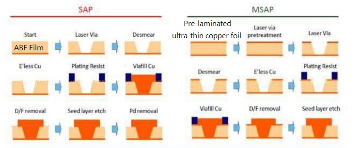
In addition, mSAP is also a cost-saving alternative for the production of fine pitch circuits: SAP semi-additive process is the process used for the production of ultrathin fine line PCBs, which requires the use of expensive ABF film. The mSAP process uses a 2-3um ultra-thin copper skin as the starting copper, which can replace the copper layer in the SAP process to simulate the production of fine circuits. The different materials used can reduce the production cost.
Advantages of the mSAP Modified Semi-Additive Process:
- Cost-saving alternative for small BGA board manufacturers.
- Suitable for production of fine pitch circuits, allowing denser conductive paths and thus saving space.
- Reduces the size of PCBs, freeing up space for other electronic components including batteries, sensors, cameras, etc.
- Short signal paths improve signal transmission on PCBs.
- Accelerate the development of miniaturization of electronic products.