
Our related videos

Knowledge
Flex sputtering composite metal thin films (Cu/Al /Graphite)
Roll-to-Roll Sputtering is a metallized film process that deposits specific materials such as metal, alloy and graphite on flexible substrates.It is an efficient, reliable and mass-produced process, which can be used to make various electrode materials and their applications.
Topnano's sputter-type conductive materials are products formed by sputtering a conductive layer on a flexible polymer plastic substrate (such as PET Film/PI Film) or a flexible metal substrate (such as copper foil/aluminum foil).
Currently it is mainly used in fields related to Flexible Electronics and Flexible Printed Circuit. It can also be used as the materials for Metal Thin Film Sensors. With the sputtering of different types of metal layers, it can be used in wearable devices (such as pressure sensors and Strain gauge) and integrated sensing components for flexible displays, etc.
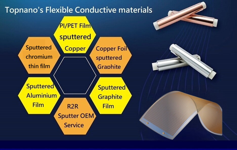
Here are some materials with conductive properties and their characteristics for reference:
1.Sputtered Copper film properties and applications
| Core Features | Technical Specifications & Competitive Advantages | Application Solutions |
| Ultra-Low Surface Roughness | Fine grain structure with minimal porosity (Ra ≤ 20nm), significantly superior to traditional Electroless (ED) or Rolled Annealed (RA) copper. | High-Speed Signal Transmission: Minimizes skin effect losses in high-frequency applications; ideal for 5G telecommunications and high-frequency sensors. |
| Fine-Line Circuit Compatibility | Uniform sputtered layer with exceptional adhesion, facilitating precise micrometer-level (μm) circuit etching. | IC Substrates & Fine-Pitch PCBs: Supports SAP/MSAP processes; enables the development of 3μm/5μm ultra-thin copper foils. |
| Multi-layer Functional Structure | Can be integrated with Horizontal Electroplating to thicken the nano-seed layer from nanometers up to 2~18μm. | Adhesiveless FCCL: Production of single/double-sided adhesiveless flexible copper clad laminates for transparent antennas and wearable electronics. |
| Superior EMI Shielding | Forms a continuous, high-density conductive layer providing excellent electromagnetic interference (EMI) blocking. | Precision Shielding Materials: Used in mobile device components, medical instrument shielding, and conductive tape substrates. |
| High Reliability Adhesion | High-energy ion bombardment in a vacuum environment creates a strong physical bond between copper atoms and PET/PI substrates. | Automotive & Aerospace: Ensures electrical stability and prevents delamination under extreme temperature fluctuations and harsh environments. |
*Topnano's sputtered copper layer is smaller than ED electrolytic copper and RA rolled copper in terms of copper crystal particles, capillary pores and surface roughness (Rq). It has a finer grain distribution range and the material surface is smoother, which is conducive to high speed transmission.
Application of sputtered copper:
Copper metal film can be made into a conductive material by plating it on a flexible substrate, and can be used as an electrode material after making circuit lines on the copper film.
Other applications include: EMI Shielding Film, Flexible Copper Clad Laminate(FCCL), FPC Antennas and other electronic component fields.
2.Sputtered Aluminium Film properties and applications
| Core Features | Technical Specifications & Competitive Advantages | Application Solutions |
| Ultra-Low Surface Roughness | Topnano’s PET substrate features a surface roughness of Ra ≤ 20nm, providing an ultra-smooth base that ensures pinhole-free aluminium deposition. | Precision Optical Films: Ideal for high-quality metallic luster finishes and advanced optical component processing. |
| Full-Spectrum EMI Shielding | Forms a continuous conductive layer that effectively blocks external electromagnetic interference (EMI) and prevents internal signal leakage. | Electronics & Communications: Used in 5G shielding components, medical devices, and precision electronic enclosures. |
| High Reflectivity & Thermal Insulation | Provides exceptionally high reflectivity across visible and infrared spectrums, effectively reflecting light and thermal radiation. | Energy & Construction: A preferred material for solar backsheet reflective layers and industrial thermal insulation membranes. |
| Superior Corrosion Resistance | Utilizing specialized vacuum sputtering processes, the aluminium layer remains stable and resistant to oxidation even in harsh chemical or humid environments. | Outdoor & Harsh Environments: Suitable for automotive components, solar panels, and specialized industrial packaging. |
Next-Generation Flexible Shielding & Barrier Expert: Topnano R2R Vacuum Sputtered Aluminium Film
In the fields of flexible electronics and precision industry, Roll-to-Roll (R2R) Vacuum Sputtering has become the high-end alternative to traditional processing methods. Topnano’s sputtered PET aluminium films, featuring ultra-low surface roughness (Ra ≤ 20nm) and a high-density metallic layer, provide critical materials for the market that combine superior optical reflection with exceptional electromagnetic shielding performance.
3.Graphite plated material properties and applications
| Material characteristics | Description |
| Electrical conductivity | Graphite has good electrical conductivity, so it can be used in various electronic devices, such as protective layers of metal substrates, film resistors, thermistors, etc. |
| High-temperature stability | Graphite has good high-temperature stability and can be used in high-temperature environments, such as high-temperature vacuum furnaces, high-temperature heat treatments, etc. |
| Low expansion coefficient | Graphite has an extremely low expansion coefficient, so it can be used in high-precision measuring instruments, manufacturing precision machinery, etc. |
| Chemical stability | Graphite has good stability to most chemicals and can be used in a variety of chemical environments. |
| Thermal Conductivity | Graphite has good thermal conductivity properties, so it can be used in various high thermal conductivity applications, such as: thermal conductive heat sinks. |
Graphite application:
It is widely used in semiconductors, electronic devices, battery materials for electric vehicles, aerospace, nuclear engineering and other fields.
Compared with artificial graphite sheets, sputtered graphite does not shed powder. In addition to the above characteristics, it can also improve wear resistance, increase surface hardness and other functions.
Topnano can sputter graphite on plastic substrates such as PET/PI Film, or on metal substrates such as copper foil, to produce high-quality graphite composite films.
*Topnano provides roll-to-roll sputtering OEM services, and stocks the above four types of target materials with conductive properties.
If you have any needs, please see "Roll-to-Roll Sputtering OEM Service" and write email to us for enquiry.
*For more Q&A about roll-to-roll sputtering, please see the FAQ at the top of the official website